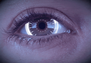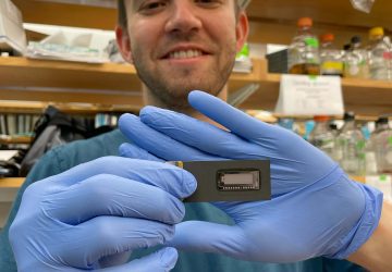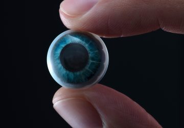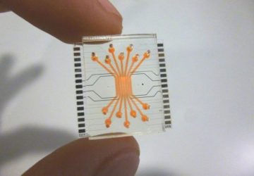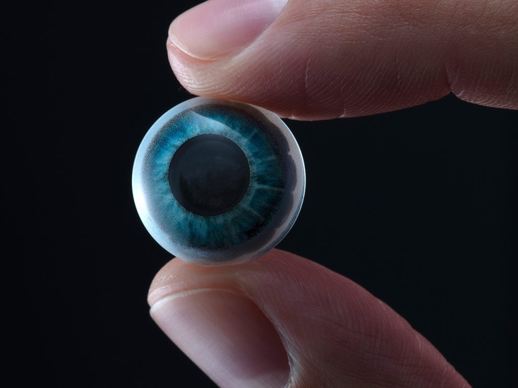
A millimeter-scale microLED display that fits onto a contact lens to provide augmented reality is, frankly, amazing, but for it to be useful it needs to know what to display. Last month at the IEEE International Solid State Circuits Conference, augmented reality contact lens startup Mojo Vision in Saratoga, Calif., reported new details of the image chip and image processing circuits that tell their display what to paint onto your retina. The two systems are seriously constrained in terms of power and area by the fact that they have to fit on a contact lens while not interfering with the wearer’s vision.
The AR lens is meant to enhance the vision of people with low-vision, Mojo Vision principal engineer Rituraj Singh told engineers at the virtual conference. About 253 million people worldwide have low vision, including those with conditions such as glaucoma, diabetic retinopathy, retinitis, pigmentosa, and macular degeneration. The goal is to help people “achieve social independence by enhancing their vision,” said Singh.
To that end, the display projects an image that enhances contrast, highlights edges, and is capable of providing some zoom. “These overlays have been identified in literature as the most helpful,” he said.
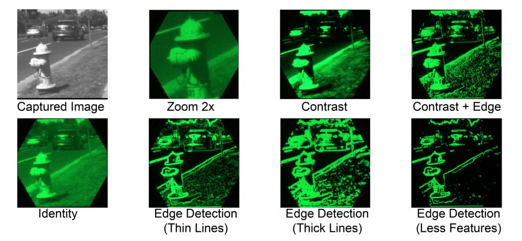
Mojo Vision’s in-contact-lens image processor is capable of zoom, contrast enhancement, and edge detection to aid those with low vision.
According to Singh, the contact lens format provided for some pretty severe design constraints. For example, the limited abilities of eye-safe batteries, housed on a flexible printed circuit board that rings the lens, mean the image processor and imager must consume little more than about 100 microwatts each. Further, the imager and the display sit squarely in the wearer’s field of vision, so they must be small enough that they don’t cast an appreciable shadow on the retina. And, because a user won’t tolerate much latency between what the imager observes and what the display produces, the image processor had to be embedded in the contact lens itself.
Mojo Vision determined that 256 x 256 monochrome pixels would be sufficient for the job. Illumination falling on each pixel would be digitized to 4-, 6-, or 8-bit values. And the image processor had to be able to perform edge detection, zoom, and contrast enhancement in addition to being programmable and tuneable.
A conventional imager architecture clearly wouldn’t do, because it would take up too much area and power, said Singh. One problem is that in a conventional imager, each column has its own analog-to-digital converter (ADC)—taking up space. The ADC and the pixel circuits take several clock cycles to reach the imager’s full resolution—consuming power.
Mojo Vision’s answer was to replace the bank of power-hungry ADCs with a set of capacitors that passively store the read out charge from the pixels. The capacitors are then sequentially selected, amplified, and fed to a shared ADC in a way designed to avoid errors. The combination saves both power and area, resulting in a 1.3 mm2 chip—perhaps the smallest of its type—that consumes no more than 61-95 microwatts depending on frame rate and bit resolution.
The image processor was kept small by sharing hardware used to produce the visual effects, and power was reduced by limiting the number of times data had to be fetched from onboard memory. The circuit consumes a maximum of 111 microwatts and occupies just 0.21 mm2 of a larger chip.
Source: www.spectrum.ieee.org

